
MENU
©2019 Guangzhou Aipu Electron Technology Co.,Ltd All rights reserved
Technology
资讯详情
ADC-based PDN deployment and place and route
Classification:
Application help
2019/02/14
Page view:
[Abstract]:
The ADC is an integral part of any system that relies on an external (analog) world to collect information for (digital) processing. From communication receivers and electronic test measurements to military and aerospace, these systems vary from application to application. The development of silicon processing technology (65 nm CMOS, 28 nm CMOS, etc.) enables high speed ADCs to span the GSPS (gigasamples per second) threshold while providing 12 or 14 bit performance. For system designers, this means a wider sampling bandwidth for digital processing. Due to environmental and cost considerations, system designers are constantly trying to reduce total power consumption. In general, ADC manufacturers recommend using a low-noise LDO (low dropout) regulator to power the GSPS (or RF sampling) ADC for maximum performance. However, this type of transmission network (PDN) is not efficient. Designers are increasingly calling for the use of switching regulators to power GSPS ADCs directly without significantly degrading ADC performance.
The solution is to carefully PDN deployment and place and route to ensure that ADC performance is not affected. This article discusses the differences between linear and switching power supplies and shows that the use of GSPS ADCs in conjunction with DC-DC converters can significantly improve system energy efficiency without affecting ADC performance. This paper explores the performance of GSPS ADCs through a combination of transmission networks and compares the cost and performance.
The PDN used by the GSPS ADC is generally recommended.
High-bandwidth, high-sampling rate ADCs (or GSPS ADCs) can have multiple power domains (AVDD, DVDD, etc.). As the size shrinks, not only does the power domain increase, but the number of different voltages required to power the ADC also increases. The new GSPS ADC design has up to seven different domains and three different voltages: 1.25 V, 2.5 V, and 3.3 V.
“...the GSPS ADC is used in conjunction with a DC-DC converter to dramatically improve system energy efficiency without affecting ADC performance.”
The increasing popularity of these power domains and various voltages is necessary to operate at these sampling rates. They ensure proper isolation between various circuit domains (sampling, clocking, digital, serializer, etc.) while optimizing performance. It is for this reason that ADC manufacturers have designed evaluation boards and recommended detailed power supply designs to ensure maximum risk reduction and maximum performance.
For example, Figure 1 shows a functional block diagram of the default PDN used by a GSPS ADC evaluation board. According to the Vita57.1 specification, the power input is supplied from the FMC (FPGA Mezzanine Card) connector.
12 V/1 A and 3.3 V/3 A power supplies. The DC-DC converter is used to bring the voltage down to a controllable level so that the LDO can be regulated without entering thermal shutdown.
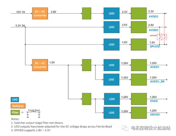
Figure 1: PDN used by the GSPS evaluation board
Obviously, this is an expensive solution with seven LDO regulators, one for each domain. This PDN may be the best performance, but certainly not the most cost-effective. System designers believe that deploying a system with multiple GSPS ADCs is very difficult.
DC–DC converter drive power supply
PDN can be further simplified by removing a single LDO that powers the 1.25 V domain. This is the most efficient and cost effective solution. The difficulty with this approach is to ensure the operational stability of the DC-DC converter so that it does not affect ADC performance. A single DC–DC converter drives the GSPS ADC. The PDN of all 1.25 V domains is shown in Figure 2.
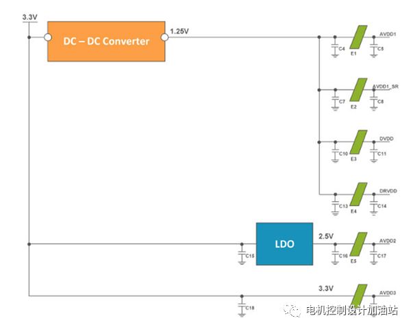
Figure 2: Powering the AD9680 with a DC-DC converter
Compare different PDNs
The two PDNs discussed above were tested. Figure 3 shows a comparison of SNR performance when using the PDN shown in Figures 1 and 2. The Nyquist zone uses the settings recommended in the data sheet.
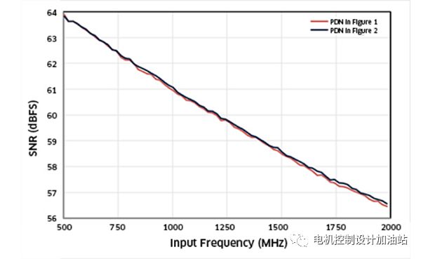
Figure 3: Performance comparison of PDN shown in Figure 1 and Figure 2
The PDN that powers the 1.25 V domain of the GSPS ADC using only the DC-DC converter shows good performance at various input frequencies. This proves that domains can be combined and powered in an efficient and cost-effective manner without losing a lot of ADC performance.
Switch spur
In addition to noise performance, due to the use of switching and magnetic components, the stray components of the DC-DC converter deployment should also be checked. At this point, it would be beneficial to use careful and careful layout techniques to reduce ground loops and ground bounce. There are many resources to help measure switching power supply noise. The sideband spurs one side of the fundamental wave and the offset frequency is the switching frequency (1.2 MHz in this example). The filter at the output of the DC-DC converter helps to reduce the switching spurs present in the output FFT, as shown in Figure 4, where the input frequency is 170 MHz.
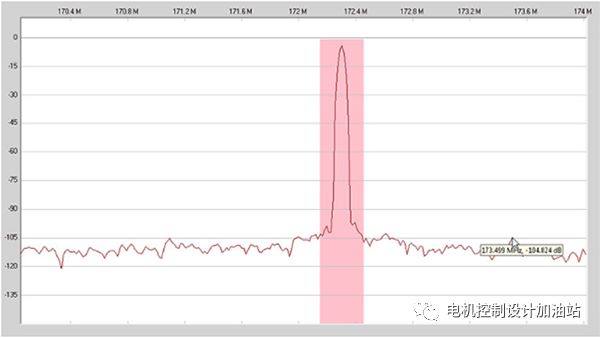
Figure 4: 1.2 MHz sideband switch spurs at 170 MHz input. Spurious level = -105 dBFS
The sideband spur level can be estimated by knowing the PSRR (power supply rejection ratio) or the power domain of the ADC.
in conclusion
The RF sampling (or GSPS) ADC digitizes the wide bandwidth and has unique advantages in system design. For these GSPS ADCs, the industry is striving to reduce the complexity, size and cost of power supply designs. The low-noise, cost-effective PDN of the DC–DC converter can power the GSPS ADC without any impact on performance.